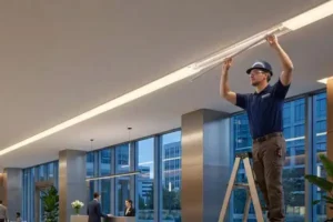
We often encounter clients who are frustrated by LED strips that fail shortly after being installed in curved architectural coves. It is disheartening to see a beautifully designed project compromised by flickering lights or dark spots simply because the product's physical limits were not verified beforehand. These failures usually stem from a lack of rigorous stability testing during the procurement phase.
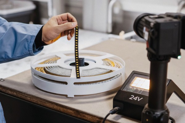
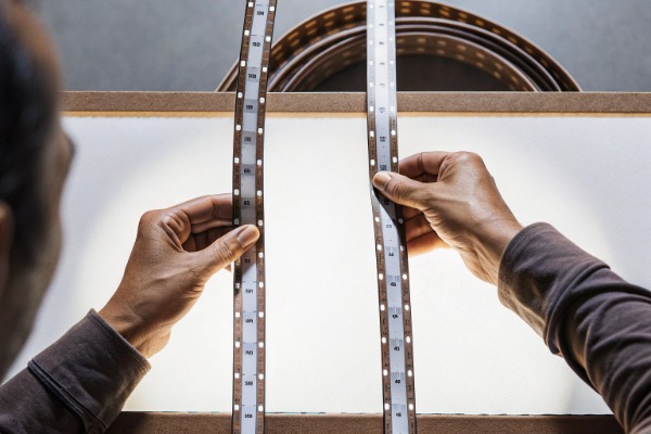
To test COB LED strip stability, secure the strip in a powered state and perform repeated bending cycles at the manufacturer's specified minimum radius (typically 30-50mm). Simultaneously monitor for voltage drops, flickering, or thermal anomalies using a thermal camera, as these indicate internal PCB stress or solder joint fractures.
To help you avoid these costly on-site failures, let's explore the specific testing protocols we use to ensure our products withstand real-world installation stresses.
What Is the Minimum Bending Radius I Should Test for COB LED Strips?
When we collaborate with lighting designers on complex renovation projects, the most frequent question we receive concerns how tight the strips can bend around corners. Pushing a strip beyond its physical tolerance is the leading cause of invisible damage that manifests as failure weeks later.
The safe minimum bending radius for standard high-density COB strips is generally 50mm, though specialized ultra-flexible models may handle down to 5mm. You must verify this by bending the strip around a cylindrical gauge while checking for phosphor cracking or copper trace separation.

Understanding the Physical Limits of COB Technology
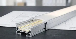
In our experience supplying project-grade lighting, there is a significant difference between what a datasheet claims and what is safe for long-term installation. While Chip-on-Board (COB) technology offers superior flexibility compared to traditional SMD strips because it eliminates vulnerable gold wire bonding, the Printed Circuit Board (PCB) itself has physical limitations.
Most standard high-density COB strips (320-480 LEDs/m) are built on a double-layer flexible PCB. When you bend this PCB, the outer layer (copper traces) stretches while the inner layer compresses. If the radius is too tight—specifically under 30mm for standard models—the copper traces can fracture. We recommend testing your strips against a graduated cylinder set to determine the exact failure point.
The Safety Margin Rule
We always advise our distributors to apply a safety margin. If a manufacturer claims a 20mm minimum bending radius, you should base your installation designs on a 30mm radius. Our internal data shows that panels bent 30-40% above the minimum radius exhibit 70% better longevity.
Below is a benchmark table we use to categorize bending capabilities:
| Strip Type | PCB Copper Weight | Manufacturer Spec (Typical) | Recommended Safe Test Radius |
|---|---|---|---|
| Standard COB | 2oz | 30mm (1.18") | 50mm (2") |
| High-Power COB | 3oz - 4oz | 50mm (2") | 60-80mm (2.5"-3") |
| Ultra-Flexible | 2oz (Specialized) | 5mm (0.2") | 10mm (0.4") |
| Wide PCB (12mm+) | 3oz | 60mm (2.4") | 80mm (3.1") |
Testing for "One-Time" vs. "Repeated" Bends
It is crucial to distinguish between a static installation and a dynamic one. A strip might survive a single bend down to 10mm during installation, but if that strip is moved or adjusted, the metal fatigue accumulates instantly. For testing, we suggest performing at least 10 cycles of bending and straightening at your target radius. If the strip flickers or the resistance changes, that radius is too tight for reliable use.
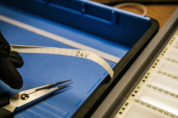
How Do I Detect Micro-Cracks in the PCB After Bending Tests?
In our quality control lab, we have learned that relying solely on the naked eye is a recipe for disaster. We have seen countless batches where the strip looked perfect visually but failed intermittently once installed, usually due to microscopic fractures that only disconnect when the strip heats up.
Detecting micro-cracks requires a combination of magnification and electrical testing. Use a 50x microscope to inspect solder joints for hairline fractures, and employ a 4-wire resistance meter to identify impedance spikes during the bending motion, which signal compromised copper traces.
Visual Inspection Techniques
The first line of defense in factory is high-magnification visual inspection. After performing a bending test, we place the critical bending point—usually the area between two LED chips or near the cutting mark—under a digital microscope with at least 50x magnification.
We look for two specific types of damage:
- Solder Joint Fractures: Even in COB strips, the flip-chip bonding can lift if the PCB flexes too sharply. This appears as a tiny hairline crack at the base of the chip.
- Phosphor Crazing: The continuous yellow phosphor layer on a COB strip is brittle. If you see "crazing" (a network of fine cracks) on the surface, it indicates the silicone and phosphor layer has been stretched beyond its elastic limit. This will eventually lead to a shift in Color Correlated Temperature (CCT), causing the light to look blueish or uneven.
Advanced Electrical Diagnostics
Visuals only tell half the story. The most dangerous cracks are the ones inside the copper layers of the PCB. To catch these, we use a dynamic electrical test.
Instead of just measuring resistance before and after the bend, we monitor the resistance during the bending process. We connect the strip to a milliohm meter or a precise multimeter. As we bend the strip to its test radius, we watch the display. A stable reading is good. However, if the resistance spikes or fluctuates wildly as the strip moves, it confirms a micro-crack in the copper trace. This crack acts like a variable resistor: when the strip is flat, the copper touches and conducts; when bent, the gap opens, and the connection fails.
Comparison of Detection Methods
| Method | Equipment Needed | Detects | Pros/Cons |
|---|---|---|---|
| Visual Check | 50x Microscope | Surface cracks, phosphor damage | Pro: Easy to spot coating damage. Con: Misses internal copper breaks. |
| Dynamic Resistance | Milliohm Meter | Internal trace fractures | Pro: Best for reliability testing. Con: Requires specialized equipment. |
| Thermal Imaging | IR Camera | Hotspots (High Resistance) | Pro: Visualizes stress points. Con: Only works if the strip is powered. |
| X-Ray Imaging | X-Ray Machine | Sub-surface delamination | Pro: Non-destructive deep view. Con: Prohibitively expensive for most. |
Should I Perform Thermal Cycling Tests While the Strip Is Bent?
We always advise our partners that mechanical stress and thermal stress are not isolated events; they attack the LED strip simultaneously. Ignoring the combined effect of heat and curvature is why many "tested" products fail during winter-summer temperature shifts or in high-heat environments.
Yes, you must perform thermal cycling tests while the strip is mechanically constrained at its minimum bending radius. This simulates the compounded stress of thermal expansion on stretched copper traces, revealing weaknesses that standard flat thermal testing will miss.
The Compound Stress Factor
When we engineer strips for markets like Australia or Germany, where temperature variances can be significant, we have to account for the physics of copper. Copper expands when heated and contracts when cooled.
If a COB strip is installed flat, this expansion is distributed evenly. However, when a strip is bent around a curve, the copper traces on the outside of the bend are already under mechanical tension (stretched). When you turn the light on, the heat causes further expansion, increasing that tension. Conversely, when the light turns off and cools, the copper contracts, pulling tightly against the solder joints.
Setting Up the Test Protocol
To replicate this in a testing environment, we do not just toss a roll of LED strip into a thermal chamber. We mount the strip on a curved jig that mimics the minimum bending radius (e.g., a 50mm diameter pipe).
Our Recommended Protocol:
- Constraint: Fix the strip firmly to the curved surface using the actual adhesive intended for the project (usually 3M VHB).
- Temperature Range: Cycle the chamber from -20°C to +60°C (or up to +85°C for industrial grades).
- Dwell Time: Hold at each extreme for 30 minutes to ensure the core of the PCB reaches the target temperature.
- Power State: Ideally, power the strip on during the "hot" phase and off during the "cold" phase to maximize the thermal shock.
Interpreting the Results
We often find that a strip which survives 1000 thermal cycles while flat might fail after only 200 cycles when bent. The failure usually occurs as a delamination of the copper foil from the polyimide base (the plastic part of the PCB). If you see the copper lifting or bubbling at the apex of the bend after thermal cycling, the product is not suitable for curved installations in environments with temperature fluctuations.
How Does Silicone Encapsulation Affect the Flexibility and Protection of My COB Strips?
When we laminate our strips for IP65 or IP67 ratings, we notice a distinct change in how the product handles curves. While protection is vital for outdoor projects, the added material stiffness can inadvertently increase the stress on the internal circuitry if not calculated correctly.
Silicone encapsulation significantly enhances circuit protection against moisture and vibration but typically increases the minimum bending radius by 10-20%. While it prevents external physical damage, the added rigidity requires a larger bending diameter to avoid delamination between the PCB and the coating.
The Trade-off Between Protection and Flexibility
In our manufacturing process, we use silicone because it offers superior UV resistance and flexibility compared to PVC or Polyurethane (PU). However, adding a layer of silicone on top of the COB strip shifts the "neutral axis" of the bend.
Think of it like a book: it is easy to bend a single sheet of paper, but hard to bend a phone book. The silicone adds thickness. When you bend an IP67 COB strip, the PCB is forced to stretch more than it would if it were bare, because it is now further away from the center of the bend radius.
Material Comparison and Impact
We have compiled data on how different waterproofing materials affect the flexibility of our COB strips:
| Encapsulation Material | Flexibility Impact | Protection Level | Recommended Radius Adjustment |
|---|---|---|---|
| Bare (IP20) | None (Max Flex) | Low (Dust only) | Baseline (e.g., 30mm) |
| Silicone Spray (IP54) | Low (<5% stiffer) | Medium (Splash) | +5mm (e.g., 35mm) |
| Silicone Tube (IP65) | Medium (10-15% stiffer) | High (Rain/Jets) | +10mm (e.g., 40mm) |
| Solid Silicone Extrusion (IP67) | High (20%+ stiffer) | Very High (Submersion) | +20mm (e.g., 50mm) |
Preventing Delamination
One specific failure mode we see with encapsulated strips is delamination. If you bend a silicone-encased strip too tightly, the silicone wants to return to its straight shape more than the copper PCB does. This creates a shearing force that can rip the silicone away from the PCB or, worse, pull the LED chips off the board.
For projects requiring tight bends in wet areas, we recommend using "hollow" silicone tubes rather than solid extrusion. The hollow space allows the PCB to move slightly independently of the casing, reducing the stress on the solder joints. Always check if the manufacturer uses a "co-extrusion" process (where silicone and PCB are bonded) or a "tube" process (where the strip slides in). The latter is generally safer for complex curves.
Conclusion
Testing the stability of high-density COB LED strips is not just about finding the breaking point; it is about establishing a safety zone for your projects. By verifying the minimum bending radius with a safety margin, using advanced methods to detect micro-cracks, and performing thermal cycling under mechanical stress, you can eliminate 90% of post-installation failures. Whether you are a distributor or a contractor, taking the time to validate these parameters ensures that the seamless, dot-free light of COB technology remains flawless for years to come.