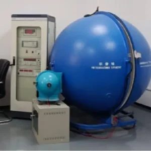
We often see clients skip basic checks, leading to project delays. Our quality control team suggests a better approach to verify sample quality immediately.
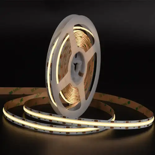
You should perform a visual inspection for solder defects, measure voltage drop and power consumption, verify color consistency against a control sample, and conduct a 48-hour burn-in test. These steps identify manufacturing flaws and ensure the COB strips meet your project's electrical and thermal specifications.
Let's break down the exact testing protocols we use in our lab to help you validate your samples.
How long should I run a burn-in test to check for early LED failure?
In our aging room, we test thousands of meters daily. Rushing this step often hides "infant mortality" defects that appear later.
Run a burn-in test for at least 48 hours at full power to catch early failures. This duration allows thermal cycles to expose weak wire bonds or defective chips. For critical projects, we recommend extending this to 96 hours to ensure absolute stability under continuous load.
Why 48 Hours is the Minimum Standard
When we develop new products, we rely on data, not guesses. The concept of "infant mortality" in electronics is real. This refers to defects that cause a product to fail very early in its life cycle. If a COB LED strip survives the first 48 to 96 hours of continuous operation, it is statistically likely to last for its rated lifespan.
You do not need complex equipment for this. Simply unroll the strip to prevent overheating (unless testing for reel heat, which is dangerous) and power it up. Watch for specific failure modes that only appear after the components heat up and expand.
What to Look For During the Test
During this period, you are not just checking if it lights up. You need to observe subtle changes.
- Flickering: This usually points to a bad wire bond inside the COB phosphor layer.
- Color Shift: If the strip turns slightly blue or yellow after 24 hours, the phosphor is degrading due to heat.
- Dead Sections: A complete blackout of a segment indicates a resistor or solder joint failure.
We use specific time benchmarks to categorize reliability.
Burn-In Duration vs. Defect Detection
| Test Duration | Defect Detection Rate | What It Reveals | Recommended For |
|---|---|---|---|
| 0 - 4 Hours | 15% | Dead on arrival, major soldering faults. | Quick visual check only. |
| 24 Hours | 60% | Overheating drivers, weak resistors. | Standard commercial orders. |
| 48 Hours | 90% | Infant mortality, phosphor stability. | Standard Project Samples. |
| 96+ Hours | 99% | Slow thermal degradation, adhesive failure. | High-end architectural projects. |
Accelerated Aging for Advanced Users
If you have limited time, you can simulate longer usage. Our engineers sometimes run samples at elevated temperatures, such as 60°C, to speed up the aging process. However, for an on-site test at your office, running the strip at room temperature for a longer period is safer and more accurate. It reflects the actual conditions your customers will face.
Do not accept a sample that has not been burned in. If a supplier sends you a "fresh" strip straight off the line without aging, you become the quality control tester. That is a risk you should not take.
What is the best way to test the flexibility of the PCB without damaging the chips?
We frequently see installers crack the phosphor layer by over-bending. Proper testing prevents costly installation mistakes and verifies PCB quality.
Wrap the COB strip around a cylinder matching its minimum bend radius specification, typically 50mm, rather than folding it. This method stresses the PCB and silicone coating evenly without cracking the internal circuitry. Check for delamination or dark spots immediately after unrolling to confirm durability.
The Cylinder Test Method
You must test flexibility objectively. Many buyers simply bend the strip back and forth in their hands. This is inconsistent. It does not replicate real installation stress.
We recommend using a cylinder or a pipe with a known diameter. For most COB strips, a 50mm (2 inch) diameter is the standard limit. Wrap the sample tightly around this object. Hold it there for 10 seconds. Then, unroll it and power it on.
If you see dark spots or flickering sections, the internal copper traces have broken. This means the PCB is too brittle or the copper layer is too thin.
Checking the Phosphor Layer
COB strips are unique because of their continuous phosphor coating. This coating is fragile. During the flexibility test, observe the surface closely.
- Cracking: Fine hairline cracks in the yellow gel will let blue light leak through. This ruins the color consistency.
- Delamination: The gel might peel away from the white PCB. This allows moisture to enter and corrodes the chips.
Torsion (Twisting) Testing
Bending is not the only stress. Installers often twist strips to fit around corners. You should perform a torsion test. Fix one end of the strip to a table. Twist the other end up to 360 degrees over a length of one meter.
This test reveals if the silicone encapsulation adheres well to the board. If it separates, the strip will fail in humid environments.
Common Flexibility Failure Modes
| Failure Sign | Root Cause | Consequence |
|---|---|---|
| Dark Spots | Broken copper trace (PCB fracture). | Permanent dead section. |
| Blue Light Leak | Cracked phosphor silicone. | Poor visual quality (color banding). |
| Gel Peeling | Poor adhesion between gel and PCB. | Water ingress and corrosion. |
| Flickering | Loose solder joint under stress. | Intermittent light failure. |
Copper Weight Matters
The flexibility depends heavily on the copper weight. We use 2oz or 3oz rolled copper for high-end strips. Cheaper alternatives use 1oz copper. Thinner copper breaks easily. When you test the sample, a stiff but durable feel usually indicates better copper content. A flimsy, paper-like feel often suggests low-quality materials that will fail during installation.
How do I measure the actual temperature rise of the strip during operation?
Our engineers always monitor heat dissipation, as it directly dictates the strip's lifespan. Guessing temperature leads to premature dimming.
Attach thermocouples to the LED pads and driver components, then run the strip for at least 4 hours to reach thermal equilibrium. The temperature rise should not exceed 50°C above ambient. Readings higher than this indicate poor thermal management, which accelerates phosphor degradation and color shift.
Setting Up the Thermal Test
You cannot rely on your hand to judge temperature. Human skin perceives 50°C as very hot, but LEDs can handle more. You need data.
Use a K-type thermocouple and a digital thermometer. Tape the sensor directly onto the yellow phosphor surface. Place another sensor on the PCB near a resistor or IC driver. These are the hottest points.
Run the test in a room with a stable temperature, ideally around 25°C. Keep the strip suspended in the air or on a standard heat sink, depending on how you plan to install it.
The 50°C Delta Rule
We follow a strict rule: the temperature rise (Delta T) must be under 50°C.
- Ambient Temp: 25°C
- Max Safe Operating Temp: 75°C
- Calculation: 75°C - 25°C = 50°C rise.
If your sample reaches 85°C or 90°C, the internal chips will degrade rapidly. The brightness will drop to 70% (L70) much faster than the promised 50,000 hours.
Thermal Runaway and Voltage Drop
Heat increases resistance. As the strip gets hotter, it might draw more current if the resistors are not properly matched. This creates a cycle called thermal runaway.
Measure the current draw at the start of the test and again after 4 hours. If the current increases significantly as the strip heats up, the design is unstable. A good design will show stable or slightly decreasing current as heat rises.
Temperature Impact on Lifespan
| Operating Temp (Case) | Estimated Lifespan (L70) | Risk Level |
|---|---|---|
| < 55°C | > 60,000 Hours | Excellent. Ideal for 24/7 use. |
| 65°C | 50,000 Hours | Standard. Good for commercial use. |
| 75°C | 30,000 Hours | Warning. Requires aluminum profile. |
| > 85°C | < 15,000 Hours | Critical Failure. Do not use. |
Color Shift Warning
High heat changes the chemical structure of the phosphor. We often see "white" strips turn blueish or greenish over time if they run too hot. If your sample gets too hot during this 4-hour test, check the color temperature again. A shift of more than 200K indicates the thermal management is insufficient for the power density.
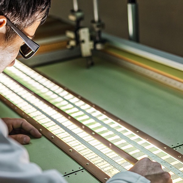
Should I cut the sample at marked points to verify soldering pad functionality?
We design cut points carefully, but poor alignment during production can make soldering impossible for your team.
Yes, you must cut a sample section to verify that the solder pads remain intact and provide sufficient surface area for reconnection. Misaligned production layers often result in cut points cutting through the circuit, rendering the remaining strip useless and complicating on-site customization.
The Hidden Risk of Misalignment
On a datasheet, cut points look perfect. In production, layers shift. The solder mask (the white paint) might cover half of the copper pad. Or, the cutting line might be printed slightly off-center.
When you cut the strip, you might find you have only a tiny sliver of copper left to solder onto. This makes installation a nightmare for your contractors. You must verify this physically.
How to Test the Cut Point
Take your scissors and cut exactly on the printed line. Now, look at both ends of the cut strip.
- Pad Size: Is there enough copper on both sides to attach a wire? You need at least 2-3mm of clean copper.
- Solder Mask: Does the white paint cover the pad? You should not have to scrape paint off to get solder to stick.
- Continuity: Use your multimeter. Check if the cut disrupted the circuit on the remaining piece. Sometimes, a cut severs a trace that runs deep inside the PCB, killing the next section.
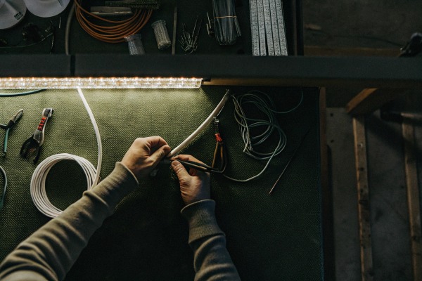
Soldering Ease
After cutting, try to solder a wire to the pad. We use tin-plated copper pads to ensure solder flows easily. If the copper is oxidized or untreated, the solder will ball up and roll off.
This test is critical for "dot-free" COB strips. The pads are often small because the chips are packed densely. If the manufacturer does not leave enough space, your installers will bridge the connections and cause short circuits.
Cut Point Evaluation Checklist
| Feature | Acceptable Standard | Red Flag (Reject Sample) |
|---|---|---|
| Pad Alignment | Centered on the cut line. | Pad is mostly on one side of the cut. |
| Copper Surface | > 2mm length available. | < 1mm (too hard to solder). |
| Surface Finish | Shiny, accepts solder instantly. | Dull, oxidized, repels solder. |
| Backing Tape | Cut cleanly with the PCB. | Peels away or bunches up at the cut. |
Connector Compatibility
Many of your customers will use solderless connectors instead of soldering. These connectors are picky. If the PCB is too thick or the pads are too narrow, the connector pins will not make contact.
Test the cut sample with the standard connectors you sell. If they do not fit securely, or if the connection is loose, you will face returns. We ensure our PCB width tolerance is tight to fit standard connectors, but you must verify this with every new supplier.
Conclusion
Testing samples on-site protects your reputation. By verifying burn-in stability, flexibility, thermal performance, and cut-point precision, you filter out low-quality products before they reach your customers. These small steps prevent massive headaches later.