When we analyze the failure rates of LED strips returned, we consistently find that the root cause is not the LED chip itself, but the foundation it sits on—the PCB. In our engineering lab, we often see competitors' "high-density" strips that look perfect on the outside but fail within months because they cut corners on the copper layer. This is a classic case of prioritizing aesthetics over electrical engineering. If you are sourcing lighting for a large commercial project, ignoring the copper weight in these dotless strips is a recipe for flickering lights, color shifts, and angry clients.
To determine if a high-density COB strip meets standards, verify it utilizes a double-layer PCB with at least 2 ounces (70μm) of copper. Check for minimal voltage drop over a 5-meter run and ensure the strip feels rigid rather than flimsy, indicating sufficient thermal mass for heat dissipation.
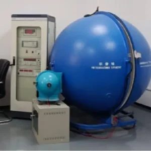
Understanding the technical specifications of the printed circuit board (PCB) is the only way to guarantee longevity. Let's explore the specific metrics and testing methods we use to ensure our products survive the rigorous demands of professional installations.
What is the recommended copper thickness for professional COB LED strips?
When we negotiate specifications with our raw material suppliers, we are adamant about copper weight because we know it is the lifeline of a COB strip. We have seen too many projects in Australia and Germany suffer because a supplier tried to pass off a standard 1oz board for a high-power application.
For professional-grade dotless COB LED strips, the recommended copper thickness is a minimum of 2 ounces (70μm) to handle the high current density. For high-power applications exceeding 15W/m or long-run installations, upgrading to 3 ounces (105μm) is essential to ensure thermal stability and prevent voltage drop.
The "Ounce" Standard Explained
In the PCB industry, copper thickness is measured in ounces (oz). This unit can be confusing if you are not familiar with it. It refers to the weight of copper spread evenly over one square foot of the board.
- 1 oz Copper: Approximately 35 micrometers (μm) thick. This is the standard for cheap, low-power decorative strips.
- 2 oz Copper: Approximately 70 micrometers (μm) thick. This is the baseline for professional COB strips.
- 3 oz Copper: Approximately 105 micrometers (μm) thick. This is used for high-end, high-wattage industrial applications.
Why COB Technology Demands More
Chip-on-Board (COB) technology is fundamentally different from traditional SMD (Surface Mounted Device) strips. In a COB strip, we pack hundreds of chips per meter—sometimes up to 480 or more—to create that seamless "dotless" effect. This density creates a massive demand for current.
If you run high current through a thin 1oz copper trace, it is like trying to force a fire hose of water through a garden straw. The resistance builds up, heat generates rapidly, and the voltage drops before it reaches the end of the strip. In our production experience, a 1oz board simply cannot handle the thermal and electrical load of a high-density COB strip without degrading quickly.
Application Suitability Table
To help you decide what you need for your specific project, we have compiled this reference table based on our manufacturing standards:
| Application Type | Power Draw (W/m) | Recommended Copper Thickness | Why? |
|---|---|---|---|
| Decorative Accent | < 10 W/m | 2 oz (Standard) | Sufficient for low heat and short runs. |
| Main Lighting (COB) | 10 - 15 W/m | 2 oz (Required) | Balances cost with necessary heat dissipation. |
| High Output / Long Run | > 15 W/m | 3 oz (Preferred) | Critical to prevent voltage drop over distance. |
| Industrial / 24-7 Use | Any | 3 oz (Heavy Duty) | Maximizes lifespan and durability. |
The Cost Reality
You might ask, "Why doesn't everyone just use 3oz copper?" The answer is cost. Moving from 1oz to 2oz copper increases the PCB material cost by roughly 60% to 100%. Moving to 3oz adds another 30-50% on top of that. Many budget manufacturers stick to 1oz to keep their prices attractive on Alibaba, hoping you won't notice the difference until after the installation is complete.
How can I verify the PCB copper weight of the samples I receive?
Whenever we receive a new batch of prototype PCBs from our fabrication partners, we don't just trust the label on the box. We verify it. As a buyer, you should do the same, even if you don't have a full laboratory at your disposal.
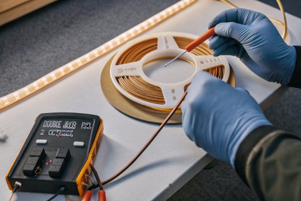
You can verify PCB copper weight by measuring the electrical resistance across a set length using a precision multimeter; 2oz copper shows roughly half the resistance of 1oz. Alternatively, perform a destructive cross-section analysis under a microscope to physically measure the copper layer thickness excluding the solder mask.
The Destructive Method: Cross-Section Analysis
This is the most accurate method, and it is what we do for final Quality Control (QC).
- Cut the Strip: Take a small sample of the LED strip.
- Polish the Edge: We use fine sandpaper to polish the cut edge until it is perfectly smooth.
- Microscope Inspection: Under a high-power microscope, you can clearly see the layers. You will see the base material (polyimide), the adhesive, and the copper layers.
- Measurement: Using the microscope's calibration software, we measure the actual thickness of the copper foil.
While you might not have a lab microscope, you can sometimes see the difference with a good magnifying glass. A 2oz or 3oz copper layer looks like a distinct, shiny metal bar, whereas a 1oz layer looks like a hairline wire.
The Non-Destructive Method: Resistance Testing
If you don't want to destroy your sample, you can use physics to your advantage. Resistance is inversely proportional to the cross-sectional area of the conductor. Thicker copper means lower resistance.
- Tools Needed: A precision multimeter.
- Process: Measure the resistance between the positive (+) pad at the start of the strip and the positive (+) pad at a specific distance (e.g., 1 meter).
- The Math: A 2oz copper strip will have significantly lower resistance than a 1oz strip of the same length and width. If you have a known "Golden Sample" (a strip you know is 2oz), you can compare the new sample against it. If the resistance is double, you have likely been sent a 1oz strip.
The Tactile "Bend" Test
This is a "field trick" we teach our sales team. Pick up the strip and gently bend it.
- Substandard (1oz): Feels like paper. It flops over easily and holds a crease sharply if you pinch it.
- Standard (2oz): Feels like cardstock. It has some spring-back and resistance when you try to bend it.
- Premium (3oz): Feels stiff, almost like a thin metal sheet. It requires intentional force to bend.
Verification Methods Comparison
Here is a quick guide on which method to use depending on your resources:
| Method | Accuracy | Equipment Needed | Pros | Cons |
|---|---|---|---|---|
| Cross-Section | High (99%) | Microscope | Definitive proof. | Destroys the sample. |
| Resistance Test | Medium (80%) | Multimeter | Non-destructive, scientific. | Requires a reference baseline. |
| Tactile/Bend | Low (50%) | Hands | Fast, free, no tools. | Subjective, requires experience. |
| Micrometer | Medium (70%) | Calipers | Quick measurement. | Hard to isolate copper from plastic. |
Why does copper thickness matter for the heat management of my LED projects?
In our R&D meetings, we constantly remind our designers that heat is the number one enemy of LEDs. We can use the most expensive chips in the world, but if the thermal path is blocked by thin copper, those chips will degrade.
Copper thickness is the primary factor in heat management because the copper layer acts as the main heat sink for the LED chips. Thicker copper traces provide a wider thermal pathway, rapidly conducting heat away from the diodes to prevent thermal degradation, color shifting, and premature failure.
The Thermal Pathway Explained
LEDs do not emit heat as infrared radiation like old incandescent bulbs; they conduct heat out through their back. In a flexible LED strip, there is no large aluminum heatsink attached to every chip. The PCB is the heatsink.
The heat travels from the LED chip $\rightarrow$ Solder Joint $\rightarrow$ Copper Foil $\rightarrow$ Air/Aluminum Profile.
If the copper foil is too thin (1oz), it creates a "thermal bottleneck." The heat cannot move away from the chip fast enough. It backs up, causing the "Junction Temperature" ($T_j$) of the LED to rise.
Consequences of High Junction Temperature
When we run accelerated aging tests in our ovens, we see exactly what happens when copper is too thin:
- Lumen Depreciation: The LEDs get dimmer much faster. A strip that should last 50,000 hours might lose 30% of its brightness in just 10,000 hours.
- Color Shift: High heat damages the phosphor coating on the LED. A crisp 4000K white light will slowly turn into a sickly blue or purple over time.
- Adhesive Failure: The heat from the copper transfers to the 3M tape on the back. If it gets too hot, the adhesive degrades, and the strip starts peeling off the ceiling.
COB Specifics: The Heat Density Problem
Dotless COB strips are particularly vulnerable because the heat source is continuous. In a traditional SMD strip, there is space between LEDs for the board to cool down. In a COB strip, it is a continuous line of heat.
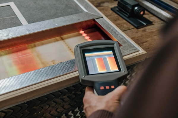
Thermal Performance Data (Estimated)
The following table illustrates the relationship between copper thickness and operating temperature based on our internal testing of a 15W/m COB strip without an external profile:
| Copper Thickness | PCB Temperature (After 1 Hour) | Risk Level | Result |
|---|---|---|---|
| 1 oz (35μm) | > 75°C | Critical | High risk of rapid decay & burn-out. |
| 2 oz (70μm) | 55°C - 60°C | Moderate | Acceptable for standard use. |
| 3 oz (105μm) | < 50°C | Low | Excellent longevity and stability. |
Note: These figures are approximate and depend on ambient temperature, but they demonstrate the trend clearly.
What are the signs that a COB strip has substandard copper thickness?
We often get calls from distributors who bought cheaper strips elsewhere and are now facing a nightmare of warranty claims. They ask us to help troubleshoot, and usually, the signs are obvious before we even open the package.
Signs of substandard copper thickness include visible dimming at the end of a 5-meter run due to voltage drop, the strip becoming too hot to touch (over 60°C) within minutes, and a flimsy, paper-like physical texture that lacks the rigidity found in high-quality, heavy-copper PCBs.
Symptom 1: The Voltage Drop Fade
The most immediate visual sign is voltage drop. Connect a 5-meter reel to power from one end only.
- The Test: Place the head (powered end) next to the tail (unpowered end).
- The Result: If the tail is visibly dimmer than the head, the copper is too thin to carry the current that distance. In a high-quality 3oz strip, the brightness should be nearly identical from start to finish.
- Why it happens: Thin copper has high resistance. As current travels down the strip, voltage is "lost" as heat. By the time it reaches the end, a 24V supply might drop to 21V or 20V, causing the LEDs to dim.
Symptom 2: The "Too Hot to Touch" Test
Power on the strip and let it run for 10 to 15 minutes. Then, carefully touch the PCB (avoiding the live solder pads).
- Good Copper: The strip will feel warm, but you can keep your finger on it comfortably. The heat is being spread out evenly.
- Bad Copper: The strip will feel intensely hot, perhaps even stinging your finger. This indicates the heat is trapped and concentrating in the copper because there isn't enough mass to dissipate it.
Symptom 3: Installation Failures
Contractors often report that cheap strips are "hard to solder." This is actually a counter-intuitive sign.
- Thick Copper: It takes a moment for the soldering iron to heat up the pad because the copper is efficiently sucking the heat away (doing its job!).
- Thin Copper: The pad heats up instantly, and sometimes the copper pad even lifts off (delaminates) from the plastic backing because the glue melts immediately. If your pads are lifting off easily during installation, the copper is likely too thin.
Troubleshooting Checklist
If you suspect your current supplier is cutting corners, use this checklist to diagnose the issue:
| Observation | Likely Cause | Recommended Action |
|---|---|---|
| Tail end is yellow/dim | Voltage Drop (Thin Copper) | Switch to 3oz PCB or power from both ends. |
| Strip curls/warps when hot | Thermal Stress (Thin Copper) | Use an aluminum profile or upgrade PCB. |
| Solder pads lift off | Poor Adhesion / Thin Foil | Reject the batch; manufacturing defect. |
| Flickering sections | Micro-cracks in Copper | Copper is too brittle/thin for bending. |
Conclusion
Determining the quality of a COB LED strip goes far beyond looking at the brightness or the price tag. The copper thickness of the PCB is the hidden backbone that dictates safety, performance, and lifespan. While 2oz copper is the industry minimum for professional results, investing in 3oz solutions for high-density applications is often the smartest business decision you can make. It prevents the headaches of voltage drop and the embarrassment of early product failures. As you source your next project, look past the light and examine the metal that makes it possible.