Every year, we see project returns that trace back to one invisible culprit: static electricity. On our production line, a single uncontrolled ESD event can silently weaken hundreds of flip-chip LEDs in a dense COB strip—damage that only shows up months later as flickering or dead spots on a finished ceiling.
To test ESD resistance of high-density dotless COB LED strips, apply standardized discharge models—Human Body Model (HBM) and Charged Device Model (CDM)—using calibrated ESD simulators per IEC 61000-4-2. Verify results by measuring forward voltage shifts, leakage current changes, and luminous uniformity before and after discharge events.
Below, I break down the exact setup, batch verification, early damage signs, and reports you should demand. Each section gives you practical steps you can use on your next project spec.
How can I properly set up an ESD test to ensure my COB LED strips meet project safety standards?
When we ship COB strips to contractors in Germany and Australia, the first question is always about reliability. A poorly set up ESD test gives false confidence, and that leads to field failures nobody wants to deal with.
To properly set up an ESD test, use a calibrated HBM or CDM simulator on an ESD-safe bench, apply contact discharge at 2000V minimum to multiple points along the strip, and measure forward voltage, leakage current, and light output before and after each event to confirm pass/fail criteria.
Choosing the Right ESD Model
Not all ESD tests are equal. The three main models each simulate a different real-world scenario. Here is a quick comparison:
| ESD Model | What It Simulates | Rise Time | Typical Test Voltage | Best For |
|---|---|---|---|---|
| HBM (Human Body Model) | A person touching the strip | ~10 ns | 2000–4000 V | Handling and installation risk |
| CDM (Charged Device Model) | The strip itself discharging | < 1 ns | 500–2000 V | Pick-and-place and packaging risk |
| IEC 61000-4-2 1 (System Level) | Real-world mixed events | ~1 ns | 4000–8000 V | Installed system immunity |
For most commercial lighting projects, HBM at 2000V is the baseline. If your strips will be handled extensively on-site, you need at least 2000V contact discharge and 4000V air discharge per IEC 61000-4-2.
Setting Up the Test Bench
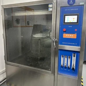
The bench itself matters more than people think. A conductive surface with proper grounding is essential. Our engineers use a horizontal coupling plane 2 connected to the ESD simulator's ground reference through a 470 kΩ resistor, following IEC 61000-4-2 guidelines.
Key setup steps:
- Place the COB strip on an insulating support 0.08 m above the ground reference plane.
- Connect the ESD simulator to a calibrated discharge network (150 pF / 330 Ω for HBM).
- Choose multiple discharge points—at least one every 500 mm along the strip—to test uniformity.
- Record ambient humidity. Below 30% RH, static charges build up much faster and test severity increases.
What to Measure Before and After
A pass/fail verdict needs data, not just a visual check. Before the first discharge, record forward voltage (Vf) 3, reverse leakage current (Ir), and luminous flux at rated current. After each discharge event, repeat those measurements. A shift of more than 5% in Vf or any measurable increase in Ir is a red flag. Luminous uniformity should stay within ±3% across the tested section.
Also inspect with a microscope. Flip-chip LEDs in high-density COB arrays (480–512 LEDs/m) are tiny. Damage can appear as micro-cracks or discoloration in the phosphor layer, invisible to the naked eye.
Why Humidity Matters
I once saw a batch pass ESD testing in summer (60% RH) and fail spectacularly in a dry winter warehouse (15% RH). The environment changes how charge accumulates. Always note and control humidity during testing. If your project site is in a dry climate, test at the lower end of humidity to reflect real conditions.
How do I verify that ESD protection remains consistent across different production batches of my dotless COB strips?
Batch-to-batch consistency is something we obsess over, because our clients in Australia run long-term projects where strips from March must match strips from September. One batch passing ESD tests means nothing if the next batch quietly falls short.
Verify batch consistency by requiring AQL-based ESD sampling on every production lot, comparing forward voltage and leakage current data across batches, and insisting on Statistical Process Control (SPC) charts from your supplier that track ESD test results over time.

Why Batches Vary
LED chips come from wafers, and wafer quality can shift between runs. The phosphor encapsulation thickness, solder joint quality, and even the FPC copper weight 4 can change slightly between batches. Each of these factors affects how well the strip handles an ESD event. A thinner phosphor layer, for example, offers less mechanical and electrical buffering.
Sampling Strategy
You cannot test every meter of every reel. Instead, use an AQL (Acceptable Quality Level) sampling plan 5. Here is a practical framework:
| Batch Size (Reels) | Sample Size (Reels) | ESD Test Points per Reel | Accept / Reject |
|---|---|---|---|
| 1–50 | 5 | 3 points (start, middle, end) | 0 fail / 1 fail = reject |
| 51–200 | 13 | 3 points | 1 fail / 2 fail = reject |
| 201–500 | 20 | 3 points | 2 fail / 3 fail = reject |
Each test point should receive at least three consecutive HBM discharges at the rated voltage. Measure Vf and Ir after each set. Compare results against your golden sample—a reference reel from a known-good batch.
Using SPC Charts
Ask your manufacturer for SPC data. A control chart plotting average forward voltage shift after ESD across batches will show you trends. Statistical Process Control (SPC) charts 6 If the mean is drifting upward over six months, something in the process is degrading—maybe a new chip supplier, maybe a change in die-attach material.
Our team reviews SPC charts monthly with our chip vendors. When we spot drift early, we can correct it before a full batch ships. This is the kind of proactive QC that separates reliable supply from gambling.
Cross-Referencing with Bin Codes
LED chips are binned by electrical and optical characteristics. If your manufacturer switches bins between batches without telling you, ESD performance can shift. Always request bin code traceability for each batch. Consistent bins mean consistent ESD behavior.
The Real-World Test
Beyond lab data, keep a few sample strips from every batch and run them on a powered aging rack for 500+ hours. Check for any premature lumen loss or color shift. Latent ESD damage from handling often shows up as accelerated aging. If batch #7 dims faster than batch #6 under the same conditions, investigate the ESD protection.
What are the early warning signs I should look for to identify ESD damage in my high-density COB installations?
On a recent project, a contractor called us about a ceiling cove that looked perfect at install but developed faint dark spots within three months. That is exactly how latent ESD damage behaves—it does not announce itself loudly.
Early warning signs of ESD damage in COB installations include localized dimming or dark spots, slight color temperature shifts in specific segments, increased flicker under dimming, elevated surface temperature on affected sections, and a gradual rise in power consumption without corresponding brightness increase.

Visible Symptoms
The most obvious sign is uneven brightness. High-density COB strips (480–512 LEDs/m) produce a smooth, dotless line of light. Any interruption in that uniformity stands out. Look for:
- Localized dimming: A section that is 10–20% dimmer than its neighbors.
- Color spots: A warm patch in a cool-white strip, or vice versa. This happens when damaged LEDs shift their emission wavelength.
- Complete dead segments: In severe cases, a group of LEDs fails entirely, creating a visible gap.
Electrical Symptoms
These are harder to spot without instruments but far more telling:
| Symptom | How to Detect | What It Means |
|---|---|---|
| Forward voltage increase (>5%) | Measure Vf with a multimeter at test pads | Junction damage from ESD |
| Leakage current rise | Reverse bias test at rated voltage | Insulation breakdown in die |
| Increased flicker at low dimming | Use a flicker meter or smartphone app | Unstable LED junctions struggling at low current |
| Higher power draw, same brightness | Compare wattage vs. lumen output | Energy wasted as heat in damaged junctions |
Thermal Red Flags
A damaged section often runs hotter. Use a thermal camera to scan the strip after 30 minutes of operation. A hot spot more than 5°C above the surrounding strip temperature is suspicious. This excess heat comes from increased resistance at damaged junctions—energy that should become light instead becomes waste heat, which further accelerates degradation.
The Timeline of Latent Damage
ESD damage is not like a blown fuse. It is more like a hairline crack in a foundation. The strip works fine at first. Over weeks or months, thermal cycling and normal operating stress widen the initial defect. This is why we always tell our clients: static damage does not break things immediately. It buries a hidden problem that slowly gets worse.
In our experience, latent ESD damage typically becomes visible within 3 to 6 months of continuous operation. By that point, the cost of replacement far exceeds the cost of proper ESD testing and handling upfront.
What to Do When You Spot Signs
If you suspect ESD damage on an installed strip:
- Photograph the affected area with a ruler for scale.
- Measure Vf and Ir at the nearest accessible solder pads.
- Record the installation date, batch number, and ambient conditions.
- Contact your supplier with this data—it is far more useful than a vague complaint.
Which specific ESD testing reports should I request from my manufacturer to guarantee long-term reliability for my commercial projects?
When we prepare documentation for our German and Australian clients, we know exactly what a sharp procurement manager will ask for. Vague claims like ">2000V ESD" on a datasheet are not enough—you need actual test reports with methodology, sample size, and raw data.
Request HBM and CDM component-level test reports per ANSI/ESDA/JEDEC JS-001 and JS-002, IEC 61000-4-2 system-level immunity reports, pre- and post-test electrical parameter data (Vf, Ir, flux), and third-party lab certification confirming the claimed ESD withstand voltage for each LED chip lot.

The Must-Have Reports
Not all ESD reports are created equal. Here is what to ask for and why:
1. Component-Level HBM/CDM Report
This report tests the bare LED chips before they are assembled onto the strip. It should follow ANSI/ESDA/JEDEC JS-001 7 (for HBM) and JS-002 (for CDM). The report must state the test voltage, number of samples, pass/fail criteria, and which classification the chips fall into (e.g., Class 1A: 250–500V, Class 1B: 500–1000V, Class 1C: 1000–2000V, Class 2: 2000–4000V). For commercial-grade COB strips, you want Class 2 or higher.
2. System-Level IEC 61000-4-2 Report
This tests the finished strip product—not just the chip. It uses contact and air discharge at specified levels. A credible report includes the test setup diagram, discharge points on the strip, number of discharges per point, and the performance criteria (A = no degradation, B = temporary degradation, C = needs reset, D = permanent damage). You want Criteria A at a minimum of ±4 kV contact and ±8 kV air discharge.
3. Pre/Post Electrical Data Sheet
This is the raw data showing Vf, Ir, and luminous flux measured on each sample before the first discharge and after the final discharge. Without this, the pass/fail verdict is just a claim. Look for Vf shift below 5% and zero increase in Ir.
Red Flags in Reports
Watch out for these signs that a report may not be trustworthy:
- No sample size stated. Testing one piece and calling it a pass is meaningless.
- No test lab accreditation. The lab should be ISO 17025 accredited for ESD testing.
- Only air discharge tested. Contact discharge is more severe and more relevant to handling. If the report only shows air discharge, ask why.
- Generic chip data used for finished strip claims. A chip-level report does not prove the assembled strip has the same ESD resistance. Assembly processes can introduce new vulnerabilities.
What a Complete Documentation Package Looks Like
| Document | Standard/Reference | Key Data Points | Who Issues It |
|---|---|---|---|
| HBM Test Report | ANSI/ESDA/JEDEC JS-001 | Voltage class, sample size, pass rate | Chip supplier or 3rd-party lab |
| CDM Test Report | ANSI/ESDA/JEDEC JS-002 9 | Voltage class, sample size, pass rate | Chip supplier or 3rd-party lab |
| IEC System-Level Report | IEC 61000-4-2 | Contact/air kV, performance criteria | 3rd-party accredited lab |
| Pre/Post Electrical Data | Internal QC procedure | Vf, Ir, flux per sample | Manufacturer QC department |
| SPC Summary (ongoing) | Internal SPC protocol | Batch-to-batch trend charts | Manufacturer QC department |
Beyond the Report: Ask the Right Questions
A report is a snapshot. For long-term reliability, also ask:
- "Do you test every incoming chip lot, or only the first qualification lot?" (You want every lot.)
- "What is your factory's ESD protection protocol 10 during assembly?" (Grounded workstations, wrist straps, ionizers, conductive flooring—all of these matter.)
- "Can you share your ESD event log from the past 12 months?" (A factory that tracks ESD events takes the issue seriously.)
In our experience, the manufacturers who can produce this documentation without hesitation are the ones running properly controlled lines. The ones who hesitate or provide incomplete data are often the ones whose strips develop issues six months into a project. Trust the data, not the marketing.
Conclusion
ESD testing is not glamorous, but it is the difference between a five-year installation and a five-month headache. Demand real data, verify across batches, watch for early signs, and your COB LED projects will last.
Footnotes
- International standard defining test methods for electrostatic discharge immunity. ↩︎
- Describes a key component in ESD test bench setup following IEC 61000-4-2 guidelines. ↩︎
- Defines a critical electrical parameter for LED performance. ↩︎
- Details technical specifications for copper thickness in flexible printed circuit boards. ↩︎
- Explains a common quality control sampling method for product inspections. ↩︎
- Explains a tool for monitoring and controlling manufacturing processes over time. ↩︎
- Standard for Human Body Model (HBM) ESD testing of integrated circuits. ↩︎
- Standard for the competence, impartiality, and consistent operation of testing and calibration laboratories. ↩︎
- Standard for Charged Device Model (CDM) ESD testing of integrated circuits. ↩︎
- Working page from the authoritative ESD Association on basic ESD control procedures and materials, replacing a 404 PDF from the same organization. ↩︎