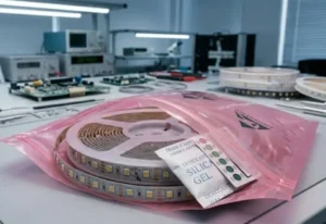
Contractors often struggle with pixelated lighting ruining sleek designs and causing client dissatisfaction. At our Shenzhen facility, we see how this frustration drives the shift toward advanced, seamless lighting solutions that solve these on-site headaches.
COB LED strips offer engineering contractors superior value through a continuous, dot-free phosphor coating that eliminates visible hotspots without deep diffusers. Their flip-chip design improves thermal dissipation and durability, reducing maintenance costs while enabling tighter bending radii for complex architectural installations compared to traditional SMD options.
Let's explore the specific technical advantages that make this switch profitable for your projects.
How does the dot-free effect of COB strips improve my project's visual finish?
You likely face client complaints about "spotted" reflections on glossy surfaces like marble or glass. When we test lighting output in our lab, we prioritize eliminating these distractions to ensure a premium aesthetic for high-end projects.
The high-density chip arrangement in COB strips creates a seamless linear light source, completely removing the pixelated "dots" inherent in SMD technology. This ensures uniform illumination on reflective materials, eliminating the need for deep aluminum profiles or heavy diffusion covers to achieve a professional finish.

When you manage a high-end renovation or a commercial fit-out, the visual quality of the lighting can make or break the final handover. Traditional Surface Mounted Device (SMD) strips, such as the common 5050 or 2835 models, feature individual LED chips spaced apart on the circuit board. Even with a high density of 120 LEDs per meter, gaps remain between the light sources.
Surface Mounted Device (SMD) 1
The Physics of Uniformity
These gaps create "hotspots"—bright points of light followed by darker spaces. In our manufacturing process, we solve this with Chip-on-Board (COB) technology. Instead of packaging chips individually, we mount hundreds of chips directly onto the PCB, often exceeding 480 chips per meter. We then cover the entire array with a continuous layer of phosphor silicone. This converts the blue LED light into white light uniformly across the entire length of the strip.
Chip-on-Board (COB) technology 2
For an engineering contractor, this means the light output is a solid, continuous line rather than a series of dots. You do not need to rely on the diffuser cover to mix the light.
Solving the "Specular Reflection" Issue
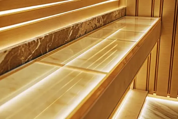
The most critical advantage appears when lighting reflective surfaces. If you install an SMD strip under a kitchen cabinet with a granite countertop or above a polished tile floor, the surface acts like a mirror. It reflects the individual dots of the LED strip, which looks cheap and unfinished.
surface acts like a mirror 3
With COB strips, the reflection is a smooth, continuous bar of light. This "dot-free" performance allows you to deliver a much higher perceived value to your client without requiring extra accessories.
Comparison of Visual Characteristics
The table below outlines the key visual differences you will notice immediately upon installation.
| Feature | Traditional SMD Strip | COB LED Strip | Impact on Project |
|---|---|---|---|
| Light Source | Point source (individual dots) | Linear source (continuous line) | COB looks more premium. |
| Beam Angle | Typically 120 degrees | Up to 180 degrees | COB covers more area evenly. |
| Reflections | Visible dots on glossy surfaces | Smooth line on glossy surfaces | COB is safe for marble/glass. |
| Diffuser Need | Requires milky/thick diffuser | Works with clear or no diffuser | COB offers cleaner aesthetics. |
Will using flexible COB strips reduce my installation time and labor costs?
Installing deep aluminum channels to hide hotspots slows down your crew and complicates joinery work. We engineer our strips to simplify this process, helping you meet tight project deadlines by reducing necessary hardware.
Yes, COB strips significantly lower labor costs by allowing the use of ultra-shallow, low-profile channels without requiring deeper cuts into cabinetry or drywall. Their uniform output removes the need for complex, multi-layered diffusion accessories, speeding up the installation process for large-scale engineering projects.

Time is the most expensive resource on any construction site. As a contractor, you know that every minute spent routing out a groove in a cabinet or waiting for a specialized deep profile to arrive eats into your margin. Traditional SMD strips often dictate the construction details because they require distance to diffuse light properly.
Eliminating Deep Channels
To hide the dots of an SMD strip, you typically need an aluminum profile that is at least 15mm deep, combined with a milky diffuser cover. This often means you have to route deep channels into joinery, which can compromise the structural integrity of thinner panels (like 16mm shelving).
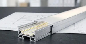
Because COB strips are naturally dot-free, you can use ultra-slim profiles—sometimes as shallow as 3mm to 5mm. In many cases, you can surface-mount the profile without it looking obtrusive. This eliminates the need for routing entirely in some applications, saving hours of carpentry labor per project.
Faster Assembly on Site
Consider the workflow for a large commercial project with hundreds of meters of linear lighting.
- Less Accessories: You do not need to source and install "high-diffusion" covers, which often reduce brightness. A standard clear or slightly frosted cover works perfectly with COB.
- Forgiving Placement: Because the beam angle is wider (180 degrees vs. 120 degrees), the placement of the strip is slightly more forgiving. You don't get harsh shadow lines if the strip isn't perfectly centered in a wide channel.
- Simplified Inventory: You can stock one type of COB strip that works for both direct view applications and hidden cove lighting, reducing the complexity of your inventory management.
Installation Cost Analysis
We have broken down the potential savings based on feedback from our contractor partners.
| Cost Factor | SMD Installation Scenario | COB Installation Scenario | Savings Potential |
|---|---|---|---|
| Profile Type | Deep profile (requires routing) | Surface or shallow profile | High (Labor & Material) |
| Carpentry Prep | High (cutting deep grooves) | Low (minimal or no cutting) | Very High (Labor) |
| Diffuser Loss | High (milky cover eats 30% light) | Low (clear cover eats 5-10%) | Efficiency Gain |
| Rework Risk | Moderate (hotspots visible) | Low (guaranteed uniformity) | Risk Reduction |
Do COB LED strips offer better thermal management for long-term reliability?
Premature LED failure damages your reputation and eats into margins through warranty calls. Our R&D team focuses heavily on heat dissipation paths to prevent these costly issues and ensure the product survives the warranty period.
heat dissipation 4
COB strips provide superior thermal management by mounting chips directly onto the PCB, creating a direct path for heat dissipation. This design lowers the junction temperature compared to SMD encased chips, significantly extending the lifespan and maintaining consistent brightness over long operational hours.

Heat is the number one enemy of LED longevity. When an LED chip gets too hot, its brightness degrades rapidly (lumen depreciation), and its color can shift. For engineering contractors, "reliability" means installing the product and never having to return to fix it.
lumen depreciation 5
Direct-to-PCB Cooling
In a traditional SMD setup, the LED chip is placed inside a plastic bracket (the "package"), bonded with gold wire, and then soldered to the PCB. The plastic package acts as a thermal insulator, trapping heat near the light source. The heat has to travel through several layers before it can dissipate into the air or the aluminum profile.
COB technology changes this architecture completely. We mount the die (the chip) directly onto the Printed Circuit Board (PCB). There is no plastic packaging and no intermediate barrier. This allows the heat to transfer instantly from the chip to the copper of the PCB.
Printed Circuit Board (PCB) 6
Reducing Voltage Drop and Heat
Because we can dissipate heat more efficiently, COB strips can run at higher densities without burning out. Furthermore, high-quality COB strips (like the ones we manufacture for project-grade orders) typically use PCBs with 2oz or 3oz copper thickness. Thicker copper not only handles heat better but also reduces voltage drop over long runs.
voltage drop 7
For you, this means you can run longer lengths of strip from a single power source with less risk of the far end being dimmer than the start. It also means the LEDs operate at a lower junction temperature, which directly correlates to a longer service life (often rated L70 > 50,000 hours).
junction temperature 8
Thermal Performance Comparison
The following table illustrates the structural differences affecting heat management.
| Component | SMD (Surface Mount Device) | COB (Chip on Board) | Thermal Result |
|---|---|---|---|
| Chip Packaging | Encased in plastic/epoxy | Direct die on PCB | COB removes insulation layers. |
| Heat Path | Chip -> Wire -> Lead -> PCB | Chip -> PCB | COB path is shorter/faster. |
| Heat Distribution | Concentrated at points | Spread linearly | COB avoids localized hot spots. |
| Failure Risk | Higher due to heat buildup | Lower due to dissipation | COB lasts longer. |
Can I bend COB strips more easily around corners than SMD options?
Snapping circuit traces during installation is a nightmare for any technician working on complex joinery. We reinforce our PCB structures to withstand the twisting and turning required in modern architectural designs without failure.
COB strips offer exceptional flexibility and a tighter bending radius because they lack the fragile gold wire bonds found in SMD packages. This structural resilience allows contractors to route lighting around sharp corners and irregular shapes without damaging the internal circuitry or causing dark spots.

Architectural designs are rarely just straight lines anymore. You are likely dealing with curved reception desks, circular coves, or intricate signage. Traditional SMD strips have a physical limitation: the rigid plastic packages soldered onto the flexible PCB.
The Flip-Chip Advantage
If you bend an SMD strip too tightly, two things often happen:
- The solder joint connecting the rigid package to the flexible PCB cracks.
- The microscopic gold wire inside the package (which connects the chip to the lead frame) snaps.
microscopic gold wire 9
Either scenario results in a "dead section" of three or six LEDs. Fixing this requires cutting out the section and soldering in a new piece—a massive headache when the strip is already glued into a profile.
COB strips use "Flip-Chip" technology. We flip the chip over and bond it directly to the board without using wire bonds. The phosphor layer also adds a level of protection. Because the chips are microscopic and there is no rigid plastic casing, the stress is distributed evenly across the flexible PCB.
Navigating Complex Shapes
You can twist and bend COB strips into shapes that would destroy an SMD strip. While you still cannot fold them flat like a piece of paper (creasing will damage the copper traces), the bending radius is significantly tighter.
This flexibility is a game-changer for:
- Signage: Creating letters or logos.
- Custom Furniture: Routing light around rounded corners of tables or desks.
- Uneven Surfaces: Adhering to textured or non-linear architectural features.
By choosing COB, you reduce the waste rate during installation. Your technicians are less likely to accidentally break the strip while maneuvering it into place, ensuring the project stays on budget and on schedule.
Conclusion
COB technology offers contractors superior aesthetics, durability, and installation speed compared to SMD. Upgrading ensures happier clients through dot-free lighting and fewer callbacks, securing your reputation for excellence in engineering projects.
converts the blue LED light 10
Footnotes
- Defines the traditional electronic assembly method contrasted with COB. ↩︎
- Explains the advanced packaging technology that eliminates lighting hotspots. ↩︎
- Explains the optical phenomenon causing unwanted reflections on glossy surfaces. ↩︎
- Details the engineering process of removing excess heat to prevent failure. ↩︎
- Authoritative definition of how LED brightness decreases over time. ↩︎
- Identifies the foundational component used to support and connect electronic parts. ↩︎
- Explains the loss of electrical potential over long circuit runs. ↩︎
- Defines the critical internal temperature metric affecting LED lifespan. ↩︎
- Describes the delicate internal connection method prone to breaking in SMDs. ↩︎
- Describes the physical process of generating white light from LEDs. ↩︎