Every time our engineering team starts a new custom LED strip project, one question keeps coming back from buyers: how do I know your factory actually designs its own PCBs KiCad 1? It is a fair question. The PCB is the backbone of every LED strip. A poorly designed circuit board causes voltage drop 2, color shift, and premature failure. The problem is real. Many suppliers claim in-house design capability, but they just modify generic boards from third-party vendors. The consequence? Your project suffers from inconsistent performance, field returns, and damaged reputation. The solution starts with knowing exactly what to ask and what to look for.
To assess a supplier's independent PCB design capability, request their engineering team credentials, review original design files such as Gerber data and schematic diagrams, ask for DFM analysis reports, evaluate their prototyping turnaround, and test their ability to explain trace routing logic and voltage drop control for your specific application.
This guide walks you through the key steps, documents, and red flags to watch for. Whether you are a distributor sourcing private-label LED strips or a contractor specifying lighting for a commercial project, these methods will help you separate capable manufacturers from resellers using off-the-shelf boards.
How do I verify if my LED strip supplier actually handles PCB design in-house?
When we receive factory audit requests from buyers in Germany or Australia, the first thing they want to see is our PCB design workstation and the engineers sitting at it. That instinct is correct. Many suppliers in this industry outsource circuit design to third-party board houses and simply assemble what arrives. The problem? They cannot adjust layouts when your project needs a specific cut length, a non-standard LED pitch, or a custom current path. The agony shows up later as flickering strips, uneven brightness, and failed site inspections.
To verify in-house PCB design, ask for a facility tour or video showing their EDA workstations, request original Gerber files with their company metadata, and have their engineers walk you through the trace routing logic and component placement rationale for a recent project.
Ask the Right Questions First
The simplest test is a conversation. Ask the supplier's engineering team why they chose a particular trace width for a 24V, 5-meter run. A capable team will explain the relationship between trace width, copper weight, current load, and acceptable voltage drop. They will reference their design rules. If the answer is "we follow industry standards" with no specifics, that is a warning sign. In our experience working with Australian contractors who need 20-meter constant-current runs, every project has unique parameters. Generic answers mean generic boards.
What to Look for During a Factory Visit or Virtual Tour
Request to see the PCB design area. Look for EDA software like Altium Designer 3, KiCad, or PADS running on dedicated workstations. Ask to see the revision history of a recent board design. Real in-house teams maintain version-controlled files. They can show you Rev A, Rev B, and explain what changed and why.
Red Flags vs. Green Flags
| Indicator | Green Flag (In-House Design) | Red Flag (Outsourced Design) |
|---|---|---|
| Engineering staff | Dedicated PCB designers on payroll | No visible design team; only assembly workers |
| Design software | Licensed EDA tools on workstations | Cannot name their design software |
| Gerber files | Files contain company-specific metadata | Files have third-party vendor watermarks |
| Design iteration | Can show revision history with change logs | Only has one "final" version |
| Technical Q&A | Explains trace routing, via placement 4, and thermal relief | Gives vague answers or defers to "the factory" |
| Custom project history | Portfolio of unique PCB layouts for different clients | All products share identical board layouts |
Check the Metadata
This is a trick many buyers miss. When you receive Gerber files, open them in a free viewer like GerberLogix. Gerber data 5 Check the file headers and layer names. In-house design teams embed their own naming conventions, project codes, and revision dates. If the metadata shows a different company name or a generic board house identifier, the supplier did not design that board.
Cross-Reference with Product Range
A supplier with real PCB design capability usually offers a wider range of LED strip configurations. They can produce strips with 60 LEDs per meter, 120 LEDs per meter, or custom pitches. They can adjust the number of resistors, change the constant-current IC layout, or modify the cut-unit length. If a supplier only offers three or four fixed configurations with no flexibility, their boards are likely purchased, not designed.
What technical documentation should I request to evaluate their PCB engineering expertise?
Our engineers maintain a full documentation library for every PCB we design, and we have learned that buyers who ask for these documents upfront are the ones who end up with the most successful projects. The problem many procurement managers face is not knowing which documents matter. They receive a product datasheet and assume that covers everything. It does not. A datasheet tells you what the product does. Engineering documentation tells you how and why it was designed that way.
Request Gerber files, schematic diagrams, BOM with component specifications, DFM analysis reports, voltage drop calculations, thermal simulation data, and test reports. These documents reveal whether a supplier engineered the PCB or simply sourced it from a third party.

The Core Document Checklist
Not all documents carry equal weight. Some are easy to fake or forward from a board house. Others require genuine engineering knowledge to produce. Here is what to request and what each document tells you.
| Document | What It Reveals | Difficulty to Fake |
|---|---|---|
| Gerber files (all layers) | Full PCB layout including trace routing, via placement, copper pours | Medium — metadata reveals origin |
| Schematic diagram | Circuit logic, component relationships, power distribution | High — requires real design knowledge |
| Bill of Materials (BOM) 6 | Component brands, values, tolerances, sourcing decisions | Low — but cross-reference with schematic reveals gaps |
| DFM analysis report | Manufacturability checks, potential production issues identified before fabrication | High — requires DFM software and engineering judgment |
| Voltage drop calculation | Expected voltage at every cut unit across full strip length | High — specific to each design, not available for generic boards |
| Thermal analysis / simulation | Heat distribution across the PCB under operating conditions | High — requires simulation tools and thermal expertise |
| Test report (electrical) | Flying probe or ICT results confirming circuit integrity | Medium — but should match the specific board revision |
Why the Schematic Diagram Matters Most
The schematic is the DNA of the PCB. schematic diagrams 7 It shows every connection, every component value, and the design intent. When our team designs a constant-current LED strip for a 10-meter architectural cove, the schematic shows the current regulation IC, the sense resistor values, and the feedback loop. If a supplier cannot provide a schematic, or provides one that does not match the physical board, they did not design it.
DFM Reports Show Process Maturity
Design for Manufacturability analysis is where engineering meets production. A proper DFM report, generated by tools like Valor NPI or similar, flags issues like insufficient annular rings, acid traps, trace-to-edge clearance violations, and solder paste stencil concerns. DFM analysis reports 8 When we run DFM checks on a new LED strip layout, we catch problems before the first panel is fabricated. This saves time and money. A supplier who can produce a DFM report is demonstrating that they control the full design-to-production pipeline.
Voltage Drop Calculations Are Project-Specific
This is one area where generic board suppliers fall short every time. Voltage drop across an LED strip depends on trace width, copper thickness, strip length, LED forward voltage, and drive current. A real PCB design team calculates this for each product and can provide data showing voltage at the first cut unit versus the last. When we work with contractors installing 15-meter runs in commercial lobbies, these calculations are critical. They determine whether the last meter matches the first meter in brightness and color temperature.
How to Cross-Reference Documents
Ask for the BOM and the schematic together. Every component on the BOM should appear in the schematic. Every component in the schematic should have a matching BOM entry with a specific manufacturer part number. Discrepancies between these two documents indicate sloppy engineering or, more likely, that the documents came from different sources.
How does a supplier's independent PCB design capability impact the long-term reliability of my project?
When we first started developing high-voltage LED strips for the European market, one of the hardest lessons came from a batch failure six months after installation. The root cause was a trace width that worked fine at room temperature but could not handle the thermal cycling in an outdoor canopy application. That experience taught us something fundamental: PCB design decisions made on day one determine product performance on day one thousand. And if the supplier did not make those decisions — if they just bought boards from someone else — they cannot diagnose or fix the problem when it appears.
A supplier's independent PCB design capability directly determines long-term reliability because it controls trace routing for thermal management, voltage stability over long runs, component selection for environmental resilience, and the ability to diagnose and resolve field failures through root-cause analysis.

Trace Routing and Thermal Performance
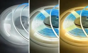
Every trace on an LED strip PCB carries current. Current generates heat. Heat accelerates LED degradation. A competent PCB designer balances trace width, copper weight, and thermal relief 9 pads to manage heat distribution across the entire strip. This is especially important for high-density strips running at 120 or 240 LEDs per meter where heat concentration around solder joints can reduce LED lifespan by 30% or more.
Voltage Stability Over Distance
Voltage drop is the most common reliability complaint in long-run LED strip installations. It causes the LEDs at the far end of the strip to appear dimmer and shift in color temperature. Independent PCB design capability means the supplier can engineer the copper pour pattern, adjust trace geometry, and place power injection points to maintain consistent voltage across the full rated length. Suppliers using generic boards have no control over these parameters.
Component Selection and Derating
A capable PCB design team selects components with appropriate derating for the target application. For example, if a strip is rated for 60°C ambient operation, the resistors and ICs should be rated for at least 85°C or higher. The BOM reflects these decisions. When we design strips for enclosed aluminum profiles used in Australian commercial fit-outs, we derate every component by at least 20% to account for thermal buildup inside the extrusion.
Root-Cause Analysis Capability
This is where independent design capability pays its biggest dividend. When a field failure occurs, a supplier who designed the PCB can trace the problem back to a specific design decision, run simulations, and implement a corrective revision. A supplier using third-party boards can only send replacements. They cannot fix the underlying issue because they do not understand or control the design.
Reliability Metrics to Track
| Reliability Factor | In-House PCB Design Impact | Generic Board Risk |
|---|---|---|
| LED lumen maintenance at 6,000 hrs | Optimized thermal path extends L70 life | Poor thermal design accelerates depreciation |
| Color consistency across strip length | Voltage drop engineered below 3% | Uncontrolled voltage drop causes visible color shift |
| Solder joint integrity under thermal cycling | Pad geometry and thermal relief designed for cycling | Standard pads crack under repeated expansion/contraction |
| Field failure diagnosis | Root-cause traced to schematic and layout | No access to design data; replacement only |
| Design iteration for new applications | Rapid layout revision for new specs | Locked into existing board geometry |
The Cost of Getting It Wrong
Testing can account for up to 30% of PCB production expense when defects are caught late. But the real cost is downstream. A failed LED strip installation in a hotel lobby or retail space means labor costs for removal, replacement product costs, project delays, and reputational damage for everyone in the supply chain. Independent PCB design capability is not a luxury. It is insurance.
Can my supplier provide rapid PCB prototyping to help me meet tight project deadlines?
In our workshop, prototype requests come in waves. A lighting designer in Melbourne sends a sketch on Monday and needs sample strips by the end of the following week for a client presentation. A German distributor wants to test a new CCT configuration before committing to a 5,000-meter order. These timelines are real. And they separate suppliers who control their PCB design process from those who depend on external board houses with their own queues and lead times.
A supplier with independent PCB design capability can typically deliver functional prototypes within 7 to 14 days because they control the design-to-fabrication pipeline internally, eliminating the delays caused by third-party design handoffs, file translation errors, and external production scheduling.

Why Speed Depends on Design Ownership
The prototyping clock starts the moment a design change is needed. If the supplier owns the PCB design, their engineer opens the file, makes the revision, runs a DFM check, and sends it to fabrication the same day. If the supplier outsources design, they must write a specification, send it to the board house, wait for questions, review the draft, request changes, and wait again. Each handoff adds one to three days. Over a typical prototype cycle, outsourced design adds a full week or more.
What a Realistic Prototype Timeline Looks Like
| Phase | In-House Design Supplier | Outsourced Design Supplier |
|---|---|---|
| Requirement review | Day 1 | Day 1–2 |
| Schematic and layout revision | Day 1–2 | Day 3–7 (waiting for external designer) |
| DFM check | Day 2 | Day 7–8 (if done at all) |
| PCB fabrication | Day 3–7 | Day 9–14 |
| SMT assembly | Day 7–9 | Day 14–17 |
| Testing and QC | Day 9–10 | Day 17–19 |
| Shipping | Day 10–14 | Day 19–24 |
The difference is significant. For project-driven buyers, this can mean the difference between winning a bid and losing it.
DFM Feedback During Prototyping
One advantage of working with a supplier who designs in-house is that DFM feedback happens in real time. When our engineers prototype a new 48V RGBW strip, they check pad clearances, via-to-trace spacing, and solder paste aperture ratios before the board goes to fabrication. This prevents the prototype from failing due to manufacturing issues, which would add another full cycle to the timeline. Suppliers who outsource design often skip this step during prototyping because it requires coordination between separate teams.
Iteration Without Starting Over
Projects rarely get the specification perfect on the first try. A contractor might test the prototype on-site and realize they need a different cut-unit length, or the dimming curve needs adjustment. A supplier with design ownership can implement these changes quickly because they understand the full circuit. They know which components to change, which traces to reroute, and which elements can stay the same. This iterative capability is critical for meeting tight deadlines.
Prototyping as a Qualification Tool
Smart buyers use the prototyping process itself as a supplier qualification exercise. How fast was the response? Did the supplier ask clarifying questions that showed genuine engineering understanding? Did the prototype match the specification? Were there any surprises? The prototyping experience tells you more about a supplier's real capability than any factory brochure or certification document.
What to Ask Before You Commit
Before placing a prototype order, ask these specific questions: What is your standard prototyping lead time from design freeze to shipment? Can you provide a DFM report before fabrication? How many design revisions are included in the prototype fee? Do you use the same production line for prototypes and mass production? The answers reveal whether the supplier has an integrated design-to-production workflow or a fragmented one that depends on external parties.
Conclusion
Assessing a supplier's independent PCB design capability comes down to evidence: original design files, engineering conversations, DFM reports, and prototyping performance. These indicators protect your project's reliability, timeline, and long-term value.
Footnotes
- Official website for KiCad, an open-source electronic design automation software suite. ↩︎
- Explains voltage drop as the decrease of electric potential along a current path. ↩︎
- Official page for Altium Designer, a leading PCB and electronic design automation software. ↩︎
- Explains vias as small holes connecting PCB layers and their importance in design. ↩︎
- Explains Gerber format as the de facto standard for PCB fabrication data. ↩︎
- Defines BOM as a structured list of all materials and components needed to build a product. ↩︎
- Defines schematic diagrams as abstract representations of circuit elements using symbols. ↩︎
- Defines Design for Manufacturability (DFM) as an engineering practice to reduce manufacturing costs and ease production. ↩︎
- Defines thermal relief pads as PCB pads connected to copper pours using thermal connections. ↩︎
- Defines root cause analysis as a method for identifying underlying causes of problems for permanent elimination. ↩︎